
|
Micromachine Summit Delegations, Americas Chief Delegate, Canada: Dan Gale
Education He graduated in 1978 from Queen's University in Kingston, Canada, with an MSc in Electrical Engineering and conducted communications research in England with Professor Peter Clarricoats (University of London, Queen Mary College) and as a research fellow (University of Surrey). Career
In 1982, he returned to join the research program in microelectronics that preceded the formation of CMC. He has authored several technical papers, journal articles and conference papers. Mr. Gale has been instrumental in building MANCEF initiatives and partnerships in Canada. Through CMC, Dan has been a major contributor to the success of COMS 2004 and linking the event to the larger Canadian Micro-Nano community.
PAST AFFILIATIONS: Forschungszentrum Karlsruhe, Karlsruhe, Germany, Laboratoire pour l' Utilisation du Rayonnement Electromagnetique, (LURE), Paris, France EDUCATION:
Sven Achenbach was born in 1969 in Juelich/Germany. He studied mechanical engineering at the University of Karlsruhe. In 1996, he was a research foundationer at the national laboratory LURE in Paris, optimizing microfabrication process technologies.
In 2004, he was appointed a Canada Research Chair in Micro and Nano Device Fabrication. He assumed the chair in early 2005, working as an Associate Professor of Electrical Engineering at the University of Saskatchewan in Saskatoon. A large portion of his work is related to the new Canadian Light Source (CLS) electron storage ring to design, build, commission and operate SyLMAND (Synchrotron Laboratory for Micro and Nano Devices), the Canadian X-ray lithography facility. Chief Delegate, Latin America: Guillermo Fernandez de la Garza President and Chief Executive Officer of the United States - Mexico Foundation for Science (FUMEC)
EDUCATION:
MAJOR PROFESSIONAL AREAS OF INTEREST:
Fernández de la Garza has worked to develop regional innovation clusters, high tech business incubation and strengthening networks, as well as facilitating innovation in medium and small businesses. He has also worked for the development of the Mexican network of Micro-Electro-Mechanical Systems, linking industry, universities and government in the definition of strategies, the development of technical and educational infrastructure, in the organization of business – university consortia to develop new MEMS based products and in the interaction with similar networks in other countries. Previously, he was advisor to UNIDO and to the governments of Brazil and Argentina in Microelectronics development strategies.
Education Mr. Fernandez de la Garza has bachelor's degrees in Engineering and in Physics from Mexico's National Autonomous University, a Master Degree in Engineering Economics from Stanford University and advanced studies in Nuclear Engineering and Business Administration from IPN and IPADE. Delegate, Latin America: Daniel Lupi
In 1999 he obtained the Master degree in Strategic Management of Innovation, ESST at the Ecole Polytechnique Fédérale de Laussane. He is international Coordinator of an international Network of "Ibero-American" Research Centers for Test and Characterization of Microelectronic Devices and Systems.
Teaching activities have included university curriculum development in instrumentation and electrical measurements. He is Professor in the National University of La Matanza, and leading several seminars for post graduate students. He was leading the national branch of IBERNET project (Microtechnologies Industrial Applications, Training and Dissemination Network in Ibero-América), European Commission (2000-2001). He was Program Chairman for several International Workshops in the field of transducers and their applications. Delegate, Latin America: Hernan Valenzuela
Career Mr. Valenzuela came from Colombia to Brazil in 1972, hired by TV Sanyo to work as a technician, and for 30 years since has worked across the telecommunications and manufacturing and foreign trade sectors. He held top plant management positions in the 1980's with Gradiente in Manaus and later headed Philips Telecommunications Service Division in São Paulo. Hernan eventually moved back to Amazônia state to offer his services in project evaluation, joint venture identification for both Brazilian and foreign companies, including Indian, Italian, French, and United States firms. Later, Hernan developed a specialty in advising companies on potential projects in the Amazônia area focused on economic and social opportunity with a small ecological footprint. Hernan's success in bringing foreign companies to the northwestern regions of Brazil has translated into advising the Superintendence of the Free Trade Zone of Manaus (SUFRAMA) on investment promotion, investment management, green energy projects, and tourism management. Today, Mr. Valenzuela is charged with implementing the creation of a Microelectronic Technology Cluster in Manaus as part of the larger economic development planning of the Brazilian Ministry of Development, Industry and Foreign Trade. Education
Chief Delegate, USA: Dr. Michael Gaitan
He is also active with international standardization activities for MEMS including the SEMI MEMS effort and is active with the International Micromachine Standardization Forum organized by Japan's Micromachine Center (MMC). Dr. Gaitan has worked to establish the MEMS Alliance, an alliance of companies, universities, and government laboratories in the Washington DC metropolitan area whose mission is to create a group that networks expertise, capabilities, and research to facilitate the development of new applications and commercialization of miniaturization technologies.
Dr. Cellucci is the author or co-author of over 98 articles on nanotechnology, laser spectroscopy, environmental disturbance control, MEMS test and measurement, and high-tech sales and marketing. Tom is on the board of Directors of the Laser Institute of America. In addition, Cellucci is a member of the Senatorial Trust - a small group of distinguished business and political leaders nominated by United States' Senators to meet on a regular basis with the highest-ranking members of the government. Tom Cellucci holds a Ph.D. in Physical Chemistry from the University of Pennsylvania, an MBA from Rutgers University, and a B.S. in Chemistry from Fordham University.
Prior to ADI, for 7 years he was the Manager of Advanced Sensor Technology for Siemens Automotive, leading a MEMS R&D facility in the US and developing suppliers for production. Preceding Siemens he was the Manager of Advance Sensor for Honeywell, Solid State Electronics Center in Plymouth Minnesota for 4 years.
Education Mr. Sulouff was educated at the University of Central Florida with BS and MS degrees in engineering materials and with executive course work at MIT Sloan.
He has been a Director at a Fortune 5 Company Division, General Manager and Vice President of medium sized businesses and President of entrepreneurial and non-profit companies. Steve received his BEng and Strategic Management PhD at Rennsselear Polytechnic Institute. He has published over 100 articles serving both the academic and practitioner communities. He has assisted firms in gaining over $200 million in equity resources in the past four years.
He is MANCEF's Founding Past President and Co-Editor of the international roadmap for MEMS and Top Down Nano technologies. |


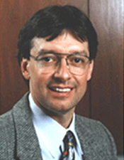

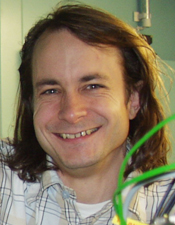 Canada Research Chair in Micro and Nano Device Fabrication, Associate Professor
of Electrical Engineering (University of Saskatchewan), Adjunct Scientist
(TRLabs, Canada), Research Scientist (Forschungszentrum Karlsruhe, Germany),
Saskatoon, Saskatchewan, Canada

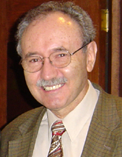 Executive Director ,The United States Mexico Foundation For Science, Mexico
City, Mexico
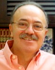 Daniel Lupi is presently the Director of the Research and Development Center
for Telecommunication, Electronics and Informatics at the National Institute
of Industrial Technology (INTI), having joined the Institution immediately
after completing his Education (National University of Buenos Aires, Electromechanical
Engineering, and electronics branch), (1975).
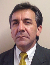 Hernan Valenzuela currently serves as the Microelectronic Program Manager
in charge of implementation of the new Microelectronic Cluster developing
under the authority of the Superintendent of the Free Trade Zone of Manaus
- SUFRAMA, a branch of the Brazilian Ministry of Development Industry and
Foreign Trade. Hernan also heads Institutional Relations for Technological
Affairs and is Senior Consultant for the Investment Promotions and Planning
Superintedant at SUFRAMA
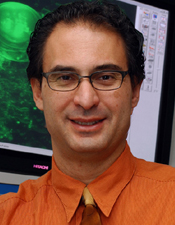 Michael Gaitan received his Ph.D. in Electrical Engineering in 1988 from
the University of Maryland, College Park. He is the Project Leader of the
MicroElectroMechanical Systems (MEMS) Project, Semiconductor Electronics
Division, Electronics and Electrical Engineering Laboratory, NIST. He directs
the MEMS Project activities in providing industry with standardized MEMS
test structures and test methods for characterizing the thermo-electro-mechanical
properties of thin-films used in IC and MEMS technologies; works with IC
foundries to improve accessibility of MEMS manufacturing; and heads research
and development of novel measurement applications of MEMS technology for
our new programs in BioElectronics and Single Molecule Manipulation and
Measurement (SM3).
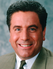 Tom Cellucci is the President and Chief Operating Officer at Zyvex, Inc
located in Richardson, Texas, USA. Zyvex has earned a reputation as the
nanotechnology leader by providing nanotechnology solutions for real-world
applications with a growing product portfolio - comprised of tools, materials
and structures.
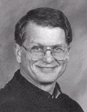

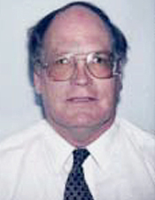 Steven Walsh is the Alfred Black Professor of Entrepreneurship and the
Co-Director of the Technology Management Center at the University of New
Mexico's Anderson School of Management, and an internationally renowned
academic and businessman.